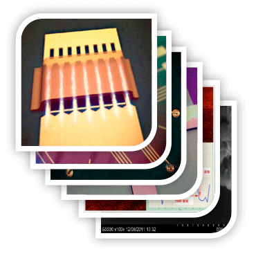
 We are pleased to announce that the Research page is now updated! 6 new projects on various topics were added. This section contains information about the recent projects on Bio-nano-electronic interfaces, GaN transistors, Nanosensor device development, Molecular nanowires, Nanomaterials and Graphene research.
CONTACTS
Head of the Center for Probe Microscopy and Nanotechnology
Doctor of Physical and Mathematical Sciences
Professor Vladimir K. Nevolin
Lead researcher
Doctor of Technical Sciences
Professor Ivan I. Bobrinetskiy
Address
124498, Moscow, Zelenograd, pass 4806, bld.5, Center for Probe Microscopy and nanotechnology (room 4125)
Phones:+7 (499) 720-89-22, +7 (499) 732-72-41
E-mail: vkn@nanotube.ru